Home >
Integrated Circuits >
Microcontrollers >
Microchip >
PIC18
PIC18F452 40-pin 32kB Microcontroller Datasheet
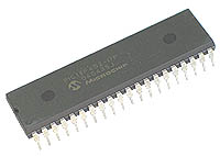
| Photograph |
|
| Product Details |
|
The Microchip PIC18F452 Microcontroller is an advanced 40-pin
8-bit PIC Microcontroller with 32kB of Flash Program Memory and
an Eight Channel 10-bit Accuracy A/D Converter.
The PIC18F452 microcontroller also contains a
USART module for RS-232 and RS-485 communication.
Together with a Master Synchronous Serial Module (MSSP) for I2C and SPI
communications. The PIC18F452 has a total of 34 I/O pins available
with individual direction control and are suitable for directly
driving LEDs.
Features
- High-Performance RISC CPU
- - Source code compatible with the PIC16 and PIC17 instruction sets
- - Linear program memory addressing to 32 Kbytes
- - DC - 40 MHz osc./clock input
- - 16-bit wide instructions, 8-bit wide data path
- - Priority levels for interrupts
- - 8 x 8 Single Cycle Hardware Multiplier
- - 32 kBytes Flash Program Memory
- - 1536 Byte RAM Data Memory
- - 256 Byte RAM Data Memory
- Peripheral Features
- - High current sink/source 25mA/25mA
- - Two 16-bit timer/counter (TMR1, TMR3)
- - One 8-bit/16-bit timer/counter with prescaler
- - One 8-bit timer/counter with 8-bit period register
- - Capture 16-bit, max. resolution 6.25ns(TCY/16)
- - Compare 16-bit, max. resolution 100ns
- - 3-wire SPI (supports all 4 SPI modes)
- - I²C Master and Slave mode
- - Addressable USART Module supports RS-485 and RS-232
- - Parallel Slave Port (PSP) module
- - Eight Channel 10-bit Analog-to-Digital Converter
- Special Microcontroller Features
- - Power-On Reset
- - Power-up Timer (PWRT) and Oscillator Start-Up Timer (OST)
- - 1,000 erase/write cycles Enhanced Flash Program Memory
- - 1,000,000 typical erase/write cycles EEPROM Data Memory
- - Watchdog Timer (WDT) with its own On-Chip RC oscillator
- - Programmable code protection
- - Power saving SLEEP mode
- - 4X Phase Lock Loop (of primary oscillator)
- - Secondary Oscillator (32kHz) clock input
- - Single supply 5V In-circuit Serial Programming via two pins
- - In-Circuit Debug (ICD)
- CMOS Technology
- - Low power, high speed CMOS FLASH technology
- - Fully Static Design
- - Wide Operating Voltage Range (2.0V to 5.5V)
- I/O and Packages
- - 34 I/O pins with individual direction control
- - 40-pin DIP
|
| Pin Layout |

|
| Pin Description |
|
Pin Number
|
Description
|
|
1
|
MCLR/VPP - Master Clear Input
|
|
2
|
RA0/AN0 - Port A
|
|
3
|
RA1/AN1 - Port A
|
|
4
|
RA2/AN2/VREF- - Port A
|
|
5
|
RA3/AN3/VREF+ - Port A
|
|
6
|
RA4/T0CKI - Port A
|
|
7
|
RA5/AN4/SS/LVDIN - Port A
|
|
8
|
RE0/RD/AN5 - Port E
|
|
9
|
RE1/WR/AN6 - Port E
|
|
10
|
RE2/CS/AN7 - Port E
|
|
11
|
Vdd - Positive Power Supply
|
|
12
|
Vss - Ground
|
|
13
|
OSC1/CLKI - Oscillator Input
|
|
14
|
OSC2/CLKO/RA6 - Port A
|
|
15
|
RC0/T1OSO/T1CKI - Port C
|
|
16
|
RC1/T1OSI/CCP2 - Port C
|
|
17
|
RC2/CCP1 - Port C
|
|
18
|
RC3/SCK/SCL - Port C
|
|
19
|
RD0/PSP0 - Port D
|
|
20
|
RD1/PSP1 - Port D
|
|
21
|
RD2/PSP2 - Port D
|
|
22
|
RD3/PSP3 - Port D
|
|
23
|
RC4/SDI/SDA - Port C
|
|
24
|
RC5/SDO - Port C
|
|
25
|
RC6/TX/CK - Port C
|
|
26
|
RC7/RX/DT - Port C
|
|
27
|
RD4/PSP4 - Port D
|
|
28
|
RD5/PSP5 - Port D
|
|
29
|
RD6/PSP6 - Port D
|
|
30
|
RD7/PSP7 - Port D
|
|
31
|
Vss - Ground
|
|
32
|
Vdd - Positive Power Supply
|
|
33
|
RB0/INT0 - Port B
|
|
34
|
RB1/INT1 - Port B
|
|
35
|
RB2/INT2 - Port B
|
|
36
|
RB3/CCP2 - Port B
|
|
37
|
RB4 - Port B
|
|
38
|
RB5/PGM - Port B
|
|
39
|
RB6/PGC - Port B
|
|
40
|
RB7/PGD - Port B
|
|
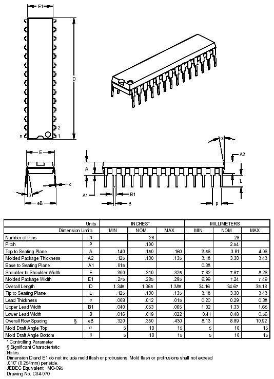
| Dimensional Drawing |
|
| Technical Data |
|
Datasheet
Application Notes
|


 Integrated Circuits