

Departments
 Integrated Circuits
Need Help
Home >
Integrated Circuits >
Microcontrollers >
Microchip >
PIC18
dsPIC30F2010 28-pin 16-bit Digital Signal Controller Datasheet
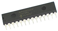
Photograph
Features
- High-Performance RISC CPU
- - Modified Harward Architecture
- - C Compiler Optimized Instruction Set Architecture
- - DC - 40 MHz osc./clock input
- - 24-bit wide instructions, 16-bit wide data path
- - Eight User Selectable Priority Levels for Each Interrupt
- - 17-bit x 17-bit Single Cycle Hardware Multiplier
- - 12 kBytes Flash Program Memory
- - 512 Byte RAM Data Memory
- - 1024 Byte EEPROM Data Memory
- Peripheral Features
- - High current sink/source 25mA/25mA
- - Three 16-bit timer/counters
- - Four 16-bit Capture Input Functions
- - Two 16-bit Compare/PWM Output Functions
- - 3-wire SPI (supports all 4 SPI modes)
- - I²C Master and Slave mode
- - Addressable USART Module
- - Six Channel 10-bit Analog-to-Digital Converter
- Motor Control PWM Features
- - Six PWM Output Channels
- - Four Duty Cycle Generators
- - Dedicated Time Base with Four Modes
- - Programmable Output Polarity
- - Dead-Time Control for Complementary Mode
- - Manual Output Control
- - Trigger for Synchronized A/D Conversions
- Quadrature Encoder Interface Module Features
- - Phase A, Phase B and Index Pulse Input
- - 16-bit Up/Down Position Counter
- - Count Direction Status
- - Position Measurement (x2 and x4) Mode
- - Programmable Digital Noise Filter on Inputs
- - Alternate 16-bit Timer/Counter Mode
- - Interrupt on Position Counter Rollover/Underflow
- Special Microcontroller Features
- - Power-On Reset
- - Power-up Timer (PWRT) and Oscillator Start-Up Timer (OST)
- - 1,000 erase/write cycles Enhanced Flash Program Memory
- - 1,000,000 typical erase/write cycles EEPROM Data Memory
- - Programmable Code Protection
- - Power Saving SLEEP mode
- CMOS Technology
- - Low power, high speed CMOS FLASH technology
- - Fully Static Design
- - Wide Operating Voltage Range (2.0V to 5.5V)
- I/O and Packages
- - 20 I/O pins with individual direction control
- - 28-pin DIP
Pin Layout

Pin Description
| Pin Number | Description |
|---|---|
| 1 | MCLR - Master Clear Reset |
| 2 | EMUD3/AN0/VREF+/CN2/RB0 - Port B |
| 3 | EMUC3/AN1/VREF-/CN3/RB1 - Port B |
| 4 | AN2/SS1/CN4/RB2 - Port B |
| 5 | AN3/INDX/CN6/RB3 - Port B |
| 6 | AN4/QEA/IC7/CN6/RB4 - Port B |
| 7 | AN5/QEB/IC8/CN7/RB5 - Port B |
| 8 | Vss - Ground |
| 9 | OSC1/CLKI - Oscillator Input |
| 10 | OSC2/CLKO/RC15 - Oscillator Output |
| 11 | EMUD1/SOSCI/T2CK/U1ATX/CN1/RC13 - Port C |
| 12 | EMUC1/SOSCO/T1CK/U1ARX/CN0/RC14 - Port C |
| 13 | RC2/CCP1/VDD1A - Port C |
| 14 | EMUD2/OSC2/IC2/INT2/RD1 - Port D |
| 15 | EMUC2/OC1/IC1/INT1/RD0 - Port D |
| 16 | FLTA/INT0/SCK1/OCFA/RE8 - Port E |
| 17 | PGD/EMUD/U1TX/SDO1/SCL/RF3 - Port F |
| 18 | PGC/EMUC/U1RX/SDI1/SDA/RF2 - Port F |
| 19 | Vss - Ground |
| 20 | Vdd - Positive Power Supply |
| 21 | PWM3H/RE5 - Port E |
| 22 | PWM3L/RE4 - Port E |
| 23 | PWM2H/RE3 - Port E |
| 24 | PWM2L/RE2 - Port E |
| 25 | PWM1H/RE1 - Port E |
| 26 | PWM1L/RE0 - Port E |
| 27 | AVSS - Analog Ground |
| 28 | AVDD - Analog Power Supply |
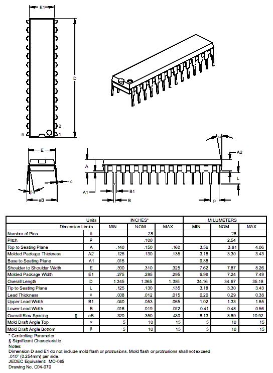
Dimensional Drawing
Technical Data
Datasheet
| Microchip Web Site - Datasheet for dsPIC30F2010 |
|
Application Notes
| Microchip Web Site - Application Notes for dsPIC30F2010 |
|